Ratchet
A few months ago I bricked my own computer during a thunderstorm. I was updating the BIOS, the low-level firmware that runs before the operating system loads, and the power cut out partway through the flash. If you lose power in the middle of writing firmware, you corrupt it. That's what happened.
When the power came back, the machine didn't. No POST, no display, nothing on screen, just fans spinning. The BIOS chip was corrupted and the board wouldn't boot.
The easy fix was to RMA the board or buy a new one. I wanted to know if I could repair it myself, so I started reading about how BIOS recovery actually works. That turned into a project I've been building since: Ratchet.
Down the repair rabbit hole
The BIOS lives on a small SPI flash chip soldered to the motherboard. To repair it you talk to that chip directly: read what's on it, back it up, erase it, and write a known-good image back. The common tool for this is a CH341A, a USB programmer that costs about three dollars on AliExpress and speaks SPI.
Getting the hardware was easy. The software was the problem. Almost everything that drives a CH341A (AsProgrammer, NeoProgrammer, the CH341A utilities) is Windows-only, built around a GUI, and close to ten years old. You download an .exe from a forum, click through an old interface, and hope it works. There's no way to script it and no structured output. I hand most of my repetitive work to agents now, and none of this could be driven by one. I was clicking through an app older than some of the chips I was trying to read.
The chip had no legs
The chip made it harder. I assumed it was an SOIC8, the eight-legged package you can clamp onto with a test clip. It wasn't. It was a WSON8. Same eight pins, but no legs. The contacts are flat pads underneath the package instead of legs on the sides, so a clip has nothing to grab.
That left two options. Desolder the chip and drop it into a socket, or hold a pin probe against the pads by hand. I didn't have a soldering iron with me, so I went with the probe.
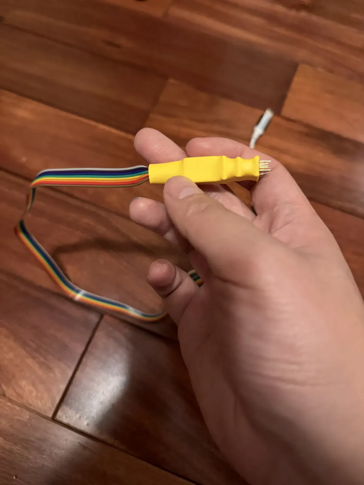
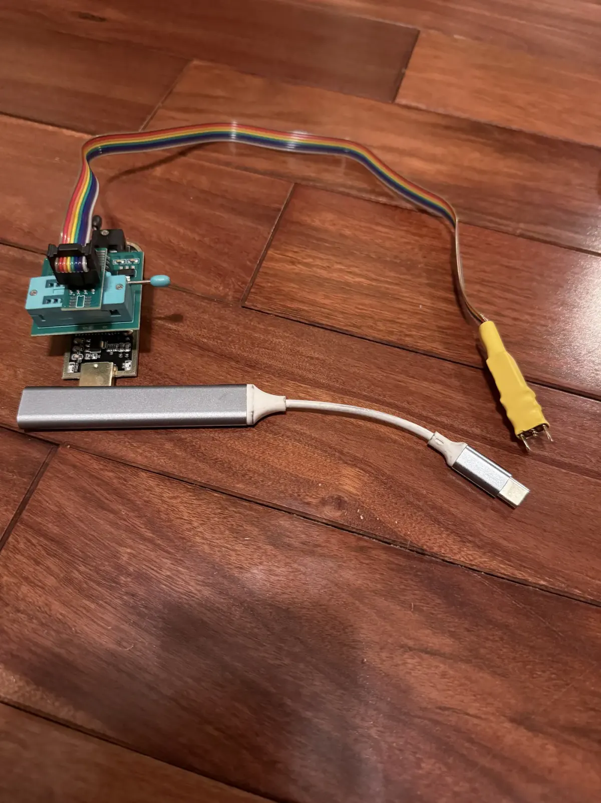
There was also a voltage problem. The chip runs at 1.8V and the CH341A puts out 3.3V, which is enough to damage it, so I needed a level-shifting adapter in between. And I only had a MacBook, which is USB-C only and can't run any of the Windows software anyway. The setup ended up being a CH341A, a 1.8V adapter, the WSON8 probe, and a USB hub to connect it all to the Mac.
How it all connects
Everything hangs off the black ZIF socket on the CH341A, the one with the little lever. Look next to it and the board has two rows printed on the silkscreen, one marked 25 and one marked 24. Those are the two chip families the programmer handles. The 25 row is for 25-series SPI flash, which is what a BIOS chip is. The 24 row is for 24-series I2C EEPROMs. For a BIOS you work off the 25 side.
The 1.8V adapter is a small board that seats into that socket on the 25 side. The CH341A drives the socket at 3.3V, which is fine for most flash but too high for a 1.8V part, so the adapter sits in the middle and steps the supply and the data lines down to 1.8V. You lift the lever, line the adapter's pins up with the 25 row, drop it in, and press the lever back down to clamp it.
The one thing you cannot get wrong is pin 1. Every part in the chain has a pin 1, and they all have to point the same way: the socket, the adapter, the ribbon cable, the clip, and the chip. The chip marks it with a dot or a notch in one corner. The ribbon cable marks it with the red stripe running down one edge. If the orientation is flipped anywhere along the line, the best case is that you read nothing back, and the worst case is that you put voltage on the wrong pins and kill the chip.
From the adapter, the rainbow ribbon cable runs out to whatever grabs the chip. For a normal SOIC8 that is a spring clip: you line the red wire up with pin 1, clamp the clip over the chip, and the sprung contacts bite onto the eight legs. For the WSON8 I had there are no legs to clamp, so the ribbon ends in a probe with eight pogo pins instead. You set the pins down onto the pads, keep the same pin-1 orientation, and hold it there. Same signal path, just held by hand instead of clipped on.
The USB-A plug on the CH341A goes into the hub, and the hub into the MacBook. So the full chain is Mac, hub, programmer, 1.8V adapter, ribbon cable, probe, chip. Once the pins make contact, Ratchet can see the chip and read its ID back, and from there you can read, back up, and write it.
Why it's called Ratchet
Holding a probe against a chip by hand is as unreliable as it sounds. The pins lose contact at the smallest movement. Losing contact during a write is the worst case, because SPI flash is written one page at a time and a half-written page is corrupt. A dropped connection mid-write would put me right back where the storm left me.
The real problem was how to write to the chip safely when the connection can drop at any moment. What worked was to back up the chip before changing anything, erase and write in fixed blocks, verify each block right after writing it, and when the connection dropped and came back, pick up from the last block that verified. Don't rewrite blocks that are already good, and don't leave one half-done.
That behavior is where the name comes from. A ratchet turns one way and holds where it is when you let go. Each block that verifies stays done, no matter how many times the probe loses contact.
Building it for agents
Once writes were safe, the original problem was still there: the tooling assumed a person clicking a mouse. So I built Ratchet to be driven programmatically, and mainly by agents.
It's written in Rust, with its own libusb layer to talk to the programmer, a database of 806 chips for identification, and full read, write, verify, and erase cycles with automatic backups before a write and verification after. The part I use most is the built-in MCP server. It exposes 31 tools over JSON-RPC: detect the chip, read it, diff it against a backup, write with retry, analyze the BIOS image. That lets an agent like Claude run the recovery. I give it the goal and it handles a failed verify or a dropped block on its own.
On the SPI-flash side it replaces AsProgrammer and NeoProgrammer, and it covers work that's normally spread across separate command-line tools like flashrom, avrdude, esptool, stm32flash, and OpenOCD, behind one interface an agent can use.
Past the BIOS
Once I could talk to one chip, I kept going. The same interface works for more than SPI flash, so I added I2C, UART, 1-Wire, JTAG, SWD, CAN, and passive SPI sniffing. Then programmers for AVR and Arduino bootloaders, 24-series and 93-series EEPROMs, ESP32 and ESP8266, and STM32, plus a logic-analyzer mode that exports to Saleae and sigrok.
The idea behind all of it is the same. Most hardware is scriptable, but the tools around it still expect a person with a mouse and a Windows machine. If you make the low-level operations structured, recoverable, and callable by an agent, a lot of hardware work that used to be tedious becomes automatable.
What a dead motherboard taught me
I'm still not sure the storm was a bad thing. I lost a working computer and a few weeks to a problem I caused. But I ended up with a tool I actually use and a much better understanding of how flash memory and these protocols work.
Buying a new board would have been faster. I'm glad I didn't. Ratchet is open source and on GitHub.